Researchers at the U.S. Department of Energy’s National Renewable Energy Laboratory (NREL) have demonstrated a new record for solar cell efficiency – 47.1%. The six-junction structured research cell required a light concentration equivalent to 143 suns. A variation of this solar cell, under standard sunlight, reached 39.2% efficiency.
The researchers, who published in Nature, suggest that a 50% efficiency solar cell with “further reduction of series resistance” was very achievable.
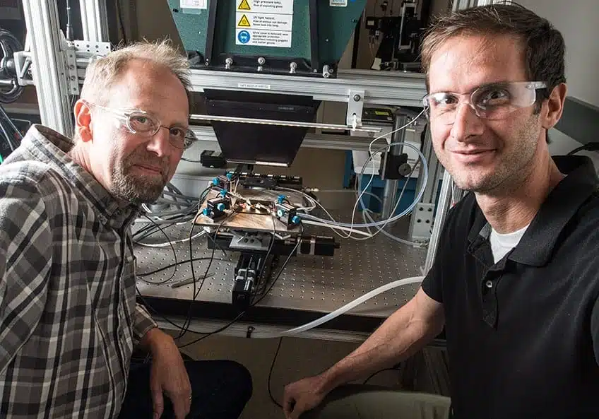
Scientists John Geisz (left) and Ryan France fabricated a solar cell that is nearly 50% efficient. Photo by Dennis Schroeder, NREL
Seemingly, more exciting than the headline value of 47.1% is the standard sunlight efficiency of 39.2%. Currently, the most efficient single-sun normal solar panel that can be bought on the open market is the SunPower X-Series near 23%, with Oxford PV and their pervovskite-silicon tandem solar module hoping to unseat them in the next couple of years. The 47.1% cell will first require a series of mirrors to increase the efficiency. Mirror structures of this nature must also track the sun, and stay within 1 degree of perpendicularity in order to focus the sunlight properly. The 39.2% cell doesn’t need this additional, expensive, hardware.
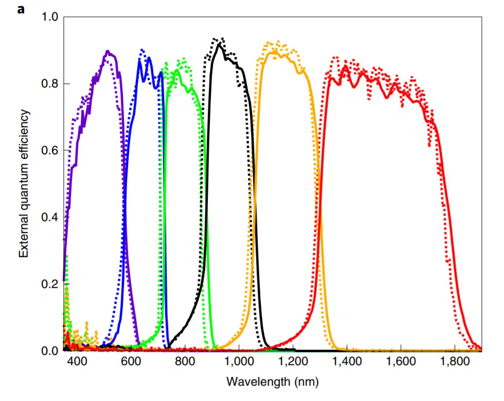
The 39.2% cell can reach this high level because the photon absorption is distributed evenly amongst the junctions. This leads to low individual voltages that add up to a very high total value. Below you see the individual layers and the specific photon wavelengths that they absorb.
These are not normal solar cells, and many other challenges exist as well. Do not expect to purchase a product of this nature anytime soon, unless you are in the military or space research (but maybe – just maybe – you’d see something something like this on a car).
The use of GaAs – Gallium Arsenide – is both the savior and challenge of solar cells of this nature. The material is very expensive relative to common silicon, and soon to scale perovskite, solar cells. As well, the manufacturing of it is relatively expensive due to the much slower vapor deposition processes used to construct the hardware. This has led to the material being used in only the most mission critical situations – like on the International Space Station or the Mars Rover. However, it seems to be the best material available to scientists to generate electricity using sunlight.
There is a long term hope though, from the same scientists at NREL, that we can scale this material. It’s just that it will take a billion dollar industry – like maybe cars or drones – to first scale with the product before it is ready for the broader electricity generation industry.
The scientists noted that, theoretically, 85% efficiency is possible for an infinite number of junctions at maximum concentration. However, using a variety of reasonable assumptions, conservative calculations suggest a 62% solar cell efficiency could be achieved at 1,000 Suns.
Each of the cell’s six junctions (the photoactive layers) is specially designed to capture light from a specific part of the solar spectrum. The device contains about 140 total layers of various III-V materials to support the performance of these junctions, and yet is three times narrower than a human hair.
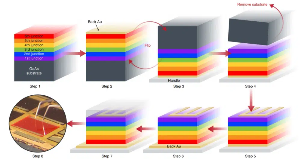
Fig. 2 | Process flow of the 6J IMM solar cell. Schematic of the fabrication steps 1–8 of the 6J IMM solar cell. Step 1, Inverted OMVPE growth of the layered structure. Step 2, Electroplate gold on the back contact of the inverted structure. Step 3, Epoxy the back of the inverted structure to a flat silicon wafer. Step 4, Remove the GaAs substrate by chemical etching. Step 5, Photolithography and deposition of NiAu front-side grids. Step 6, Mesa isolation by chemical etching down to the back gold. Step 7, Thermal deposition of a MgF2/ZnS/MgF2/ZnS anti-reflective coating. Step 8, Solar cell characterization. Step 8 shows an actual photograph of a 0.1-cm2 concentrator cell glowing under forward bias.
The solar cell is built layer by layer, with the materials layered in order of the highest bandgap junction and ends with the lowest bandgap junction. A more detailed construction process is noted above.
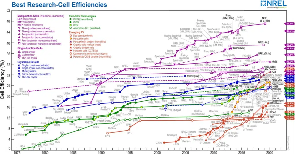
As can be seen in the famous NREL research-cell efficiency chart, way up in the top right corner is the new record – “NREL (6-J, 143x)”. And directly below it, you see NREL (6-J), representing the standard sunlight record. To the right of either of them, on the vertical axis, is the record efficiency values.
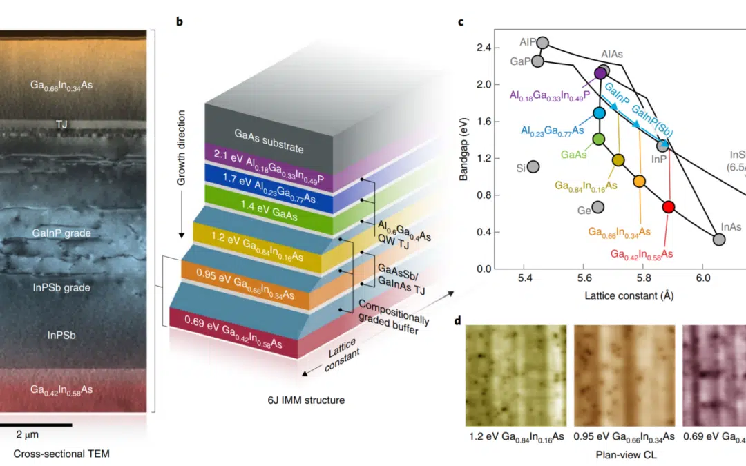
A very technical description of the header image on this article from the journal publication: Fig. 1 | Description of the 6J IMM solar cell structure. a, A 220 reflection diffraction contrast TEM image cross-sectional expansion of selected layers. b, Simplified 6J IMM structure schematic. The junction absorber thicknesses are approximately 1.2, 2.6, 1.6, 3.0, 3.2 and 2.2 µm, respectively, from the top. The layer structure is shown in greater detail in Supplementary Fig. 1. c, Bandgap versus lattice constant for the 6J IMM semiconductor design. d, Plan-view cathodoluminescence (CL) images of metamorphic GaInAs junctions. The CL images have an area of 65 × 65 µm2. The TDDs are approximately 106 cm–2 or lower for all three metamorphic junctions.